How LED Strips Are Made: Inside an SMT Production and Silicone Extrusion Line
- 2026-09-30 17:39
- /
- Arraystar LED
The quality gap between cheap LED strip and reliable product isn't visible in a glossy listing - it's decided on the SMT line, in the solder process, binning, aging test and QC that buyers almost never see. Understanding how strip is actually made - from PCB and chip placement through reflow soldering, SOB/COB encapsulation, testing and binning - tells you what to ask a factory and why two strips with identical-looking specs behave differently. Tour the process mentally and you'll spec what matters: consistent solder, binned LEDs, sealed construction and burn-in testing.

From Bare PCB to Finished Reel: the Production Flow
LED strip manufacture is a surface-mount electronics process. It starts with a flexible printed circuit board (FPCB) - the copper circuit on a polyimide substrate, designed with the pad layout for the LED density and any driver ICs. Solder paste is stencil-printed onto the pads, pick-and-place machines mount the LED packages (and resistors, and ICs for addressable strip), and the board passes through a reflow oven that melts the paste into permanent solder joints.
After soldering, the strip is tested electrically, then may get an encapsulation (IP-rated silicone extrusion/tube for waterproof versions), is cut into reels, labeled and aged. Every stage is a quality lever - and the stages buyers can't see (solder profile, binning, burn-in) are precisely where cheap and premium strip diverge.
SMT Placement and Reflow Soldering Quality
Pick-and-place accuracy and the reflow temperature profile determine solder joint quality. A well-controlled reflow profile heats and cools per the solder paste spec, producing shiny, fully-wetted joints; a rushed or poorly profiled line creates cold/dry joints, tombstoned components and solder bridges - defects that cause intermittent failures, dead pixels and early field failures, especially in addressable strip with many ICs.
Modern high-density products like the tunable SOB strip at 560 LEDs/m demand precise placement and tight process control - at that density even minor placement or soldering errors create visible gaps. Watching a reel come off a well-run SMT line with automated optical inspection (AOI) tells you more about reliability than any datasheet.
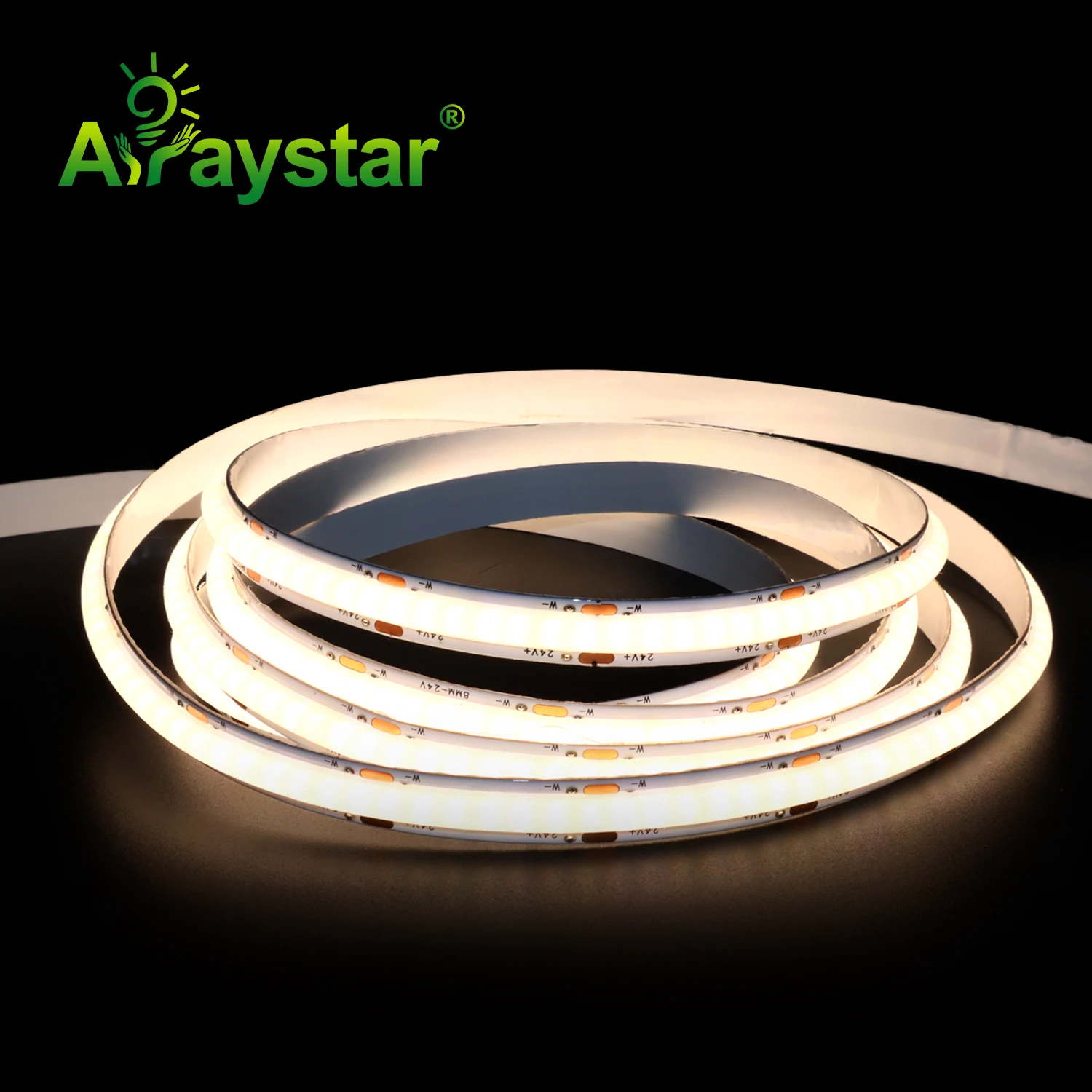
Where strip quality is actually decided.
| Stage | What it determines | Cheap vs premium tell |
|---|---|---|
| FPCB design | Copper weight, pad layout, heat path | Thin copper = heat/drop issues |
| Solder paste & printing | Joint foundation | Stencil quality, paste handling |
| Pick-and-place | Component position | AOI vs no inspection |
| Reflow profile | Solder joint integrity | Cold joints/tombstones if rushed |
| Binning & aging | Color/flux consistency, infant failures | Binned + burn-in vs untested |
COB and SOB Encapsulation
Conventional SMD strip places discrete LED packages; COB (chip-on-board) mounts bare LED chips directly on the board and coats them in a continuous phosphor layer, producing the seamless dot-free emitting surface. SOB and similar processes apply an integrated silicone/phosphor body that further protects and diffuses the chips - the construction behind slim, dense, sealed products.
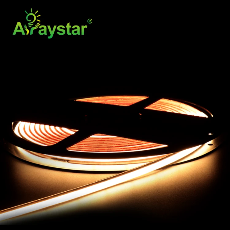
An 8x4mm IP20 240-LED/m SOB strip shows the slim indoor form the process enables, while a tunable 8mm SOB strip at 560 LEDs/m delivers high-density tunable-white light. The encapsulation process matters for both appearance (continuity, no dots) and protection - well-controlled silicone application avoids bubbles, delamination and uneven phosphor that cause color mottling.
Binning, Testing and Aging (Burn-In)
LEDs come off production with natural variation in color temperature, brightness and forward voltage; binning sorts them into tight groups so a reel - and a project - is consistent. Unbinned cheap strip mixes bins, which is why one reel can look warmer or brighter than the next. Premium production bins tightly and matches reels per order.
- Require tight color/flux binning so reels match within a project.
- Ask about AOI and electrical test coverage after reflow.
- Burn-in/aging catches infant-mortality failures before shipping.
- For IP-rated strip, inspect encapsulation for bubbles/delamination.
- Verify rated density, CCT and CRI by measurement, not label only.
- Consistent copper weight supports heat dissipation and low voltage drop.
Aging (powering reels for hours under load) weeds out infant failures - components that would otherwise die in the first weeks on your project. Factories that skip burn-in ship those early failures to you. When auditing a supplier, ask to see the SMT line, AOI station, binning process and aging racks; a factory that genuinely controls these will show them proudly.
What a Buyer Should Actually Audit
Spec sheets describe intent; the line proves capability. On a factory visit or audit, look for controlled reflow profiles with temperature logs, automated optical inspection, documented binning, burn-in/aging racks, IP encapsulation controls and incoming chip quality (reputable LED brands). The combination predicts field reliability far better than price per meter - which is why two visually identical strips can have wildly different failure rates.
Recommended Products
Frequently Asked Questions
How are LED strip lights manufactured?
A flexible PCB is stencil-printed with solder paste, pick-and-place machines mount LEDs (and resistors/ICs), and the board goes through a reflow oven to form solder joints. It's then electrically tested, optionally encapsulated (silicone tube/extrusion or COB/SOB phosphor body for waterproof/seamless versions), binned for consistency, burn-in aged, cut into reels and labeled.
What is the difference between SMD, COB and SOB LED strip?
SMD mounts discrete LED packages on the board; COB bonds bare chips directly and coats them in a continuous phosphor layer for a seamless dot-free surface; SOB applies an integrated silicone/phosphor body that protects and diffuses the chips in slim dense formats (e.g. 8x4mm 240 or 8mm 560 LED/m). COB/SOB give smoother light and better encapsulation control.
Why do two LED strips with the same specs differ in quality?
Differences hidden in manufacturing: copper/PCB quality, solder paste and reflow profile (cold joints/tombstones), pick-and-place accuracy and AOI, LED binning (color/brightness consistency), and burn-in aging to catch infant failures. Cheap strip skips inspection, tight binning and aging, so reels mismatch and fail early despite identical-looking labels.
What is LED binning and why does it matter?
LEDs naturally vary in color temperature, brightness and voltage after production; binning sorts them into tight groups. Tight binning ensures reels match within a project so there are no warmer/brighter sections, while unbinned cheap strip mixes groups and shows visible color variation. Specify tight binning and reel matching for consistent installations.
What should I check when auditing an LED strip factory?
Look for controlled reflow profiles with temperature logs, automated optical inspection (AOI), documented tight binning, burn-in/aging racks, clean IP encapsulation (no bubbles/delamination), adequate copper PCB weight, and reputable LED chip brands. These predict field reliability far better than price - a factory that controls them will show the SMT line, AOI and aging areas openly.
Need help with your LED project?
Get factory-direct pricing, free samples and engineering support within 24 hours.
Email: info@arraystarled.com | Phone: +86-0755-2103-6746 | WhatsApp: 0086 1581 8514 077
Need to size your power supply? Use our LED Strip Power Calculator to find the right driver in seconds.